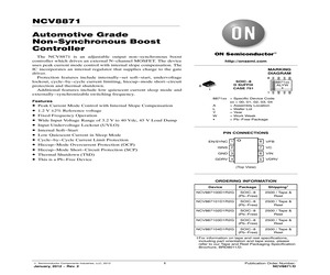
1xx = Specific Device Code xx = 00, 01, 02, 03, 04 A = Assembly Location L = Wafer Lot Y = Year W = Work Week G = Pb-Free Package PIN CONNECTIONS EN/SYNC 1 8 VFB ISNS 2 7 VC GND 3 6 VIN GDRV 4 5 VDRV (Top View) ORDERING INFORMATION Device Package Shipping NCV887100D1R2G SOIC-8 (Pb-Free) 2500 / Tape & Reel NCV887101D1R2G SOIC-8 (Pb-Free) 2500 / Tape & Reel NCV887102D1R2G SOIC-8 (Pb-Free) 2500 / Tape & Reel NCV887103D1R2G SOIC-8 (Pb-Free) 2500 / Tape & Reel NCV887104D1R2G SOIC-8 (Pb-Free) 2500 / Tape & Reel For information on tape and reel specifications, including part orientation and tape sizes, please refer to our Tape and Reel Packaging Specification Brochure, BRD8011/D. (c) Semiconductor Components Industries, LLC, 2013 October, 2013 - Rev. 5 1 Publication Order Number: NCV8871/D NCV8871 6 TEMP VDRV FAULT LOGIC EN/SYNC SYNC 1 OSC SC VC 5 CLK 7 PWM EN/ 4 2 CL + RC DRIVE LOGIC CSA 3 CDRV VDRV Cg L D Vo Q GDRV ISNS GND Co RSNS RF1 SCP CC Vg VIN 8 Gm SS VFB RF2 Vref Figure 1. Simplified Block Diag
 12 Pages, 138 KB, Original
1xx = Specific Device Code xx = 00, 01, 02, 03, 04 A = Assembly Location L = Wafer Lot Y = Year W = Work Week G = Pb-Free Package PIN CONNECTIONS EN/SYNC 1 8 VFB ISNS 2 7 VC GND 3 6 VIN GDRV 4 5 VDRV (Top View) ORDERING INFORMATION Device Package Shipping NCV887100D1R2G SOIC-8 (Pb-Free) 2500 / Tape & Reel NCV887101D1R2G SOIC-8 (Pb-Free) 2500 / Tape & Reel NCV887102D1R2G SOIC-8 (Pb-Free) 2500 / Tape & Reel NCV887103D1R2G SOIC-8 (Pb-Free) 2500 / Tape & Reel NCV887104D1R2G SOIC-8 (Pb-Free) 2500 / Tape & Reel For information on tape and reel specifications, including part orientation and tape sizes, please refer to our Tape and Reel Packaging Specification Brochure, BRD8011/D. (c) Semiconductor Components Industries, LLC, 2012 January, 2012 - Rev. 2 1 Publication Order Number: NCV8871/D NCV8871 6 TEMP VDRV FAULT LOGIC EN/SYNC SYNC 1 OSC SC VC 5 CLK 7 PWM EN/ 4 2 CL + RC DRIVE LOGIC CSA 3 CDRV VDRV Cg L D Vo Q GDRV ISNS GND Co RSNS RF1 SCP CC Vg VIN 8 Gm SS VFB RF2 Vref Figure 1. Simplified Block Diag
 12 Pages, 133 KB, Original
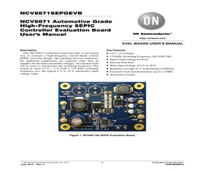
-90.9KHRCT-ND R5 RES 10.0K OHM 1/10W 1% 0603 SMD MCR03EZPFX1002 RHM10.0KHCT-ND R6 RES 10.0 OHM 1/10W 1% 0603 SMD RC0603FR-0710RL 311-10.0HRCT-ND R7 RES 715 OHM 1/10W 1% 0603 SMD CRCW0603715RFKEA 541-715HCT-ND U1 ON SEMI Non-Sync Boost Controller NCV887100 NCV887100D1R2G http://onsemi.com 6 NCV8871SEPGEVB PCB LAYOUT Figure 6. Top View Figure 7. Bottom View http://onsemi.com 7 NCV8871SEPGEVB ON Semiconductor and are registered trademarks of Semiconductor Components Industries, LLC (SCILLC). SCILLC owns the rights to a number of patents, trademarks, copyrights, trade secrets, and other intellectual property. A listing of SCILLC's product/patent coverage may be accessed at www.onsemi.com/site/pdf/Patent-Marking.pdf. SCILLC reserves the right to make changes without further notice to any products herein. SCILLC makes no warranty, representation or guarantee regarding the suitability of its products for any particular purpose, nor does SCILLC assume any liability arising out of the application or use o
 8 Pages, 623 KB, Original
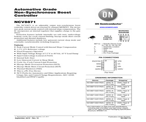
1xx = Specific Device Code xx = 00, 01, 02, 03, 04 A = Assembly Location L = Wafer Lot Y = Year W = Work Week G = Pb-Free Package PIN CONNECTIONS EN/SYNC 1 8 VFB ISNS 2 7 VC GND 3 6 VIN GDRV 4 5 VDRV (Top View) ORDERING INFORMATION Device Package Shipping NCV887100D1R2G SOIC-8 (Pb-Free) 2500 / Tape & Reel NCV887101D1R2G SOIC-8 (Pb-Free) 2500 / Tape & Reel NCV887102D1R2G SOIC-8 (Pb-Free) 2500 / Tape & Reel NCV887103D1R2G SOIC-8 (Pb-Free) 2500 / Tape & Reel NCV887104D1R2G SOIC-8 (Pb-Free) 2500 / Tape & Reel For information on tape and reel specifications, including part orientation and tape sizes, please refer to our Tape and Reel Packaging Specification Brochure, BRD8011/D. (c) Semiconductor Components Industries, LLC, 2017 October, 2018 - Rev. 14 1 Publication Order Number: NCV8871/D NCV8871 6 TEMP VDRV FAULT LOGIC EN/SYNC SYNC 1 OSC SC VC 5 CLK 7 PWM EN/ 4 2 CL + RC DRIVE LOGIC CSA 3 CDRV VDRV Cg L D Vo Q GDRV ISNS GND Co RSNS RF1 SCP CC Vg VIN 8 Gm SS VFB RF2 Vref Figure 1. Simplified Block Dia
 17 Pages, 202 KB, Original
1xx = Specific Device Code xx = 00, 01, 02, 03, 04 A = Assembly Location L = Wafer Lot Y = Year W = Work Week G = Pb-Free Package PIN CONNECTIONS EN/SYNC 1 8 VFB ISNS 2 7 VC GND 3 6 VIN GDRV 4 5 VDRV (Top View) ORDERING INFORMATION Device Package Shipping NCV887100D1R2G SOIC-8 (Pb-Free) 2500 / Tape & Reel NCV887101D1R2G SOIC-8 (Pb-Free) 2500 / Tape & Reel NCV887102D1R2G SOIC-8 (Pb-Free) 2500 / Tape & Reel NCV887103D1R2G SOIC-8 (Pb-Free) 2500 / Tape & Reel NCV887104D1R2G SOIC-8 (Pb-Free) 2500 / Tape & Reel NCV887105D1R2G SOIC-8 (Pb-Free) 2500 / Tape & Reel For information on tape and reel specifications, including part orientation and tape sizes, please refer to our Tape and Reel Packaging Specification Brochure, BRD8011/D. (c) Semiconductor Components Industries, LLC, 2017 September, 2019 - Rev. 16 1 Publication Order Number: NCV8871/D NCV8871 6 TEMP VDRV FAULT LOGIC EN/SYNC SYNC 1 OSC SC VC 5 CLK 7 PWM EN/ 4 2 CL + RC DRIVE LOGIC CSA 3 CDRV VDRV Cg L D Vo Q GDRV ISNS GND Co RSNS RF1 SCP CC Vg VI
 19 Pages, 367 KB, Original
-90.9KHRCT-ND R5 RES 10.0K OHM 1/10W 1% 0603 SMD MCR03EZPFX1002 RHM10.0KHCT-ND R6 RES 10.0 OHM 1/10W 1% 0603 SMD RC0603FR-0710RL 311-10.0HRCT-ND R7 RES 715 OHM 1/10W 1% 0603 SMD CRCW0603715RFKEA 541-715HCT-ND U1 ON SEMI Non-Sync Boost Controller NCV887100 NCV887100D1R2G http://onsemi.com 6 NCV8871SEPGEVB PCB LAYOUT Figure 6. Top View Figure 7. Bottom View http://onsemi.com 7 NCV8871SEPGEVB ON Semiconductor and are registered trademarks of Semiconductor Components Industries, LLC (SCILLC). SCILLC owns the rights to a number of patents, trademarks, copyrights, trade secrets, and other intellectual property. A listing of SCILLC's product/patent coverage may be accessed at www.onsemi.com/site/pdf/Patent-Marking.pdf. SCILLC reserves the right to make changes without further notice to any products herein. SCILLC makes no warranty, representation or guarantee regarding the suitability of its products for any particular purpose, nor does SCILLC assume any liability arising out of the application or use o
 9 Pages, 629 KB, Original
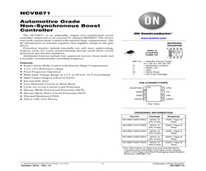
1xx = Specific Device Code xx = 00, 01, 02, 03, 04 A = Assembly Location L = Wafer Lot Y = Year W = Work Week G = Pb-Free Package PIN CONNECTIONS EN/SYNC 1 8 VFB ISNS 2 7 VC GND 3 6 VIN GDRV 4 5 VDRV (Top View) ORDERING INFORMATION Device Package Shipping NCV887100D1R2G SOIC-8 (Pb-Free) 2500 / Tape & Reel NCV887101D1R2G SOIC-8 (Pb-Free) 2500 / Tape & Reel NCV887102D1R2G SOIC-8 (Pb-Free) 2500 / Tape & Reel NCV887103D1R2G SOIC-8 (Pb-Free) 2500 / Tape & Reel NCV887104D1R2G SOIC-8 (Pb-Free) 2500 / Tape & Reel For information on tape and reel specifications, including part orientation and tape sizes, please refer to our Tape and Reel Packaging Specification Brochure, BRD8011/D. (c) Semiconductor Components Industries, LLC, 2017 October, 2018 - Rev. 14 1 Publication Order Number: NCV8871/D NCV8871 6 TEMP VDRV FAULT LOGIC EN/SYNC SYNC 1 OSC SC VC 5 CLK 7 PWM EN/ 4 2 CL + RC DRIVE LOGIC CSA 3 CDRV VDRV Cg L D Vo Q GDRV ISNS GND Co RSNS RF1 SCP CC Vg VIN 8 Gm SS VFB RF2 Vref Figure 1. Simplified Block Dia
 18 Pages, 218 KB, Original


